

【研究成果】2013年
研究成果57
Tip-Enhanced Raman Investigation of Extremely Localized Semiconductor-to-Metal Transition of a Carbon Nanotube
Yoshito Okuno, Yuika Saito, Satoshi Kawata, and Prabhat Verma
PRL 111, 216101 (2013)
The electronic properties of single walled carbon nanotubes (SWNTs) can change with a slight deformation, such as the one caused by the pressure of one SWNT crossing over the other in an ‘‘X’’ shape. The effect, however, is extremely localized. We present a tip-enhanced Raman investigation of the extremely localized semiconductor-to-metal transition of SWNTs in such a situation, where we can see how the Fano interaction, which is a Raman signature of metallic behavior, grows towards the junction and is localized within a few nanometers of its vicinity. After exploring the deconvoluted components of the G-band Raman mode, we were able to reveal the change in electronic properties of a SWNT at extremely high spatial resolution along its length.
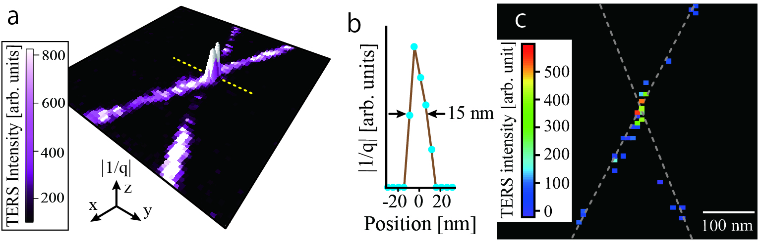
(a) A TERS image of two carbon nanotubes crossing each other in “X” shape (X-CNT sample), where the x-y plane indicates the sample plane, the color represents TERS intensity of the G+ mode in accordance with the color bar shown on the left, and the z axis shows the value of the Fano parameter |1/q|, which corresponds to the degree of semiconductor-to-metal transition. (b) A line profile of |1/q| along the yellow dashed line in (a). (c) White dashed lines depict the location of the nanotubes in the X-CNT sample, whereas the colored spots indicate the TERS intensity of a new Raman mode centered at 1607 cm-1, which arise due to the local reduction of radial symmetry, in accordance with the color bar on the left.