
Entrepreneurial/Productization Project
Entrepreneurial/Productization Project
In order to realize its mission of "creation of innovation," the Photonics Center is inviting researchers to come up with ideas for business startups and productization using photonics-related technology. Outstanding ideas will receive various forms of support from the Center. Applicants to this Project are screened by external screening committee members.[Proposal requirements]
- Proposal to realize business startup / productizationmust be achievable within two years.
- Proposal must be for business startups / productization related to photonics.
Selected proposals [Fiscal 2012]
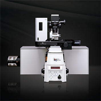 Commercialization of tip-enhanced Raman scattering microscope
- The project succeeded in product development of tip-enhanced Raman scattering microscope that utilizes light intensity enhancement by plasmon resonance. The product is now to be sold from a startup company. The technology has been under basic research for 20 years. The manufacturing technique of sharp nano-structured metal probes is the key technology.
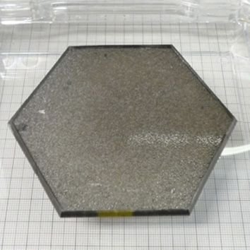
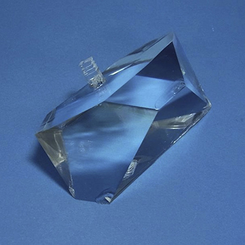 Development of wavelength conversion crystals for UV light sources (CLBO)
- Using high-quality CLBO crystal growth technology, the project successfully extended the lifetime of crystal devices. At present, preparations are being made to set up a venture business within the Photonics Center to start producing what is being called Osaka-CLBO by the end of fiscal 2014. Through partnerships with manufacturers of lasers and laser beam machines, the project aims to develop UV lasers and UV laser beam machines using CLBO crystals.
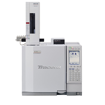 Productization of gas chromatograph systems
- Together with Shimadzu Corporation, one of the member companies, this project pursued applied research on plasma photonics to develop the Tracera gas chromatograph, which features significantly enhanced sensitivity and is now marketed throughout the world by Shimadzu Corporation. The system is throughout the world by Shimadzu Corporation. The system is capable of handling more samples than conventional detection methods with high sensitivity.
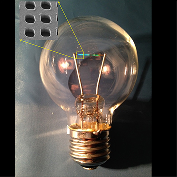 Development of eco lamps
- This project succeeded in developing incandescent lamps that can regulate thermal radiation spectra. They demonstrated that spectra would change depending on the size of tiny holes made on the surface of the incandescent lamp filament. Our goal is to realize more efficient full-spectrum light sources.
Selected proposals [Fiscal 2013]
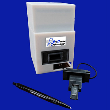 Commercialization of a Portable Electrochemical Luminescence Device
- The Photonics Center has developed a commercial version of a Portable Electrochemical Luminescence Device in partnership with Biodevice Technology, Ltd. It is suitable for use in both chemical- and bio-sensors, cell measurement, and in research on antioxidant or luminescent materials. The use of electrochemical luminescence gives the device a large detection range with high sensitivity and high signal-to-noise ratio for counting photons. In conjunction with Osaka University’s microfluidic chip design technology, the device can be customized to suit the measurement target and has potential for further business development.
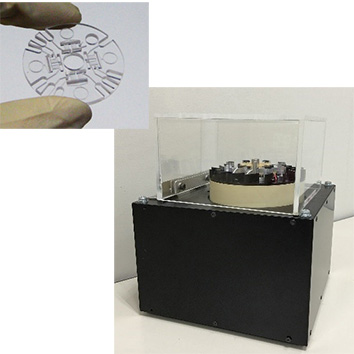 A Rapid and Easy POCT System Using Optics and PCR Technology to Detect Pathogens and Infectious Diseases
- A Rapid and Easy POCT System Using Optics and PCR Technology to Detect Pathogens and Infectious Diseases A rapid and highly sensitive polymerase chain reaction (PCR) point-of care testing (POCT) system was realized using a patented technology of centrifugation-assisted thermal convection. The system performs on-chip DNA amplification when the user simply injects a fluid specimen. Used in medical settings or other workplace environments, such as food-processing factories and restaurants, this system enables rapid highly sensitive detection and diagnosis of a variety of pathogens, including methicillin-resistant staphylococcus aureus (MRSA), influenza and norovirus, and enterohemmorhagic E. coli.
 The World’s Highest Quality GaN Wafers for Improved Characteristics of Nitride Devices
- Perfect (i.e., distortion-free and strain-free) gallium nitride (GaN) crystals that have been nonexistent outside of silicon crystals were successfully grown for the first time using a liquid phase epitaxy process on GaN in a sodium flux. High quality GaN wafers can be used to implement optical devices such as LEDs for high-intensity lighting and laser diodes with high output power in the red-to-ultraviolet range, including green lasers that are indispensable for laser light shows; power devices having less than one-tenth the power loss of silicon devices; and energy-saving optoelectronic devices such as ultrahigh-speed transistors capable of achieving one-thousand times the speed and transmission capacity of cell phones.